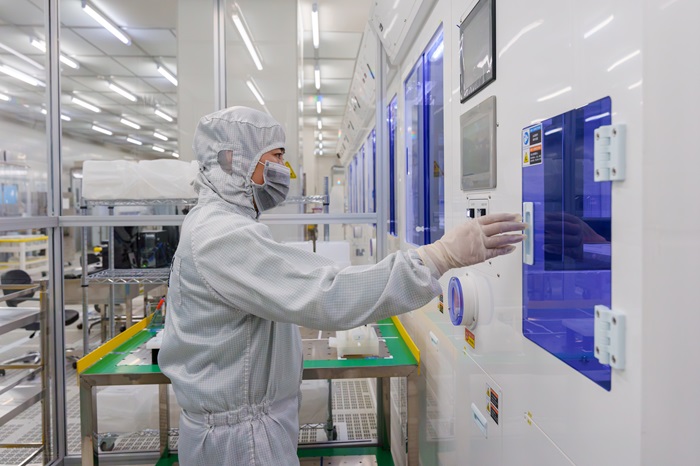
1. Key Summary
- China has succeeded in challenging the monopolistic position of the Dutch company ASML.
- The Harbin Institute of Technology research team's successful development of '13.5nm extreme ultraviolet (EUV) light source technology' marks a major step towards the localization of lithography equipment, a core component in semiconductor production.
2. What is Lithography Equipment?
- Definition: Lithography equipment is a machine that uses an extreme ultraviolet (EUV) light source to etch circuit patterns onto semiconductor wafers.
- Necessity: It is essential for manufacturing ultra-fine semiconductors below 10 nanometers.
- Current Situation: The Dutch company ASML has a monopoly on this technology, preventing China from importing it due to U.S. export restrictions.
3. China's Technological Leap
3.1. Introduction of LDP Technology
- Technological Innovation:
- The Harbin Institute of Technology adopted the Laser-induced Discharge Plasma (LDP) method.
- This method is superior in efficiency compared to ASML's existing Laser Produced Plasma (LPP) method.
- Advantages:
- Directly converts electrical energy into plasma to generate extreme ultraviolet light.
- High energy conversion efficiency and low power consumption.
- Cost-effective and has relatively lower technical complexity.
- Reduces external dependence (can operate with Chinese-made chips).
3.2. Achievement
- Awarded the 1st prize at the 2024 Heilongjiang Provincial Science and Technology Innovation Conference.
4. ASML vs. China's Harbin Institute of Technology
| Category | Netherlands ASML | China Harbin Institute of Technology |
|---|---|---|
| Technology Used | LPP Method | LDP Method |
| Required Resources | High-performance lasers and FPGA chips (dependent on imports) | Direct use of electrical energy (domestic technology) |
| Efficiency | Relatively low | High energy conversion rate |
| Power Consumption | High | Low |
| Cost | High Cost | Low Cost |
5. Future Challenges
- Despite the technological advancements of Professor Zhao's team, two major challenges remain:
- Parameter Optimization: Needs to improve technology efficiency and stability.
- Discharge Time Issue: Needs to maintain stable output over long periods.
- Some experts still point out the output limitations of LDP technology.
6. Implications and Ripple Effects
6.1. New Opportunities for China's Semiconductor Industry
- Potential to alleviate China's technology dependency due to U.S. restrictions on semiconductor equipment exports.
- Securing the basic technology for the development of domestic lithography equipment strengthens self-reliance.
6.2. Changes in the Global Semiconductor Competition Landscape
- Signals a potential shift away from the ASML-centered monopoly system.
- If successful in localizing EUV technology, China could make a new leap in the global semiconductor market.
7. Summary
- China's successful development of 13.5nm EUV lithography technology is not only a short-term technological leap but also carries significant economic and political implications in the long run.
- If the technology is perfected and moves into the production phase, it will be a critical turning point in strengthening China's semiconductor industry's independence and competitiveness in the global market.
Keywords: China, Semiconductor, Lithography Equipment, EUV, ASML Monopoly, Localization, LDP Technology, Harbin Institute of Technology, Professor Zhao Yongpeng, Technological Innovation.
*Source URL:
https://www.choicenews.co.kr/news/articleView.html?idxno=141642


