● Samsung Pushes Chiplet Powered Physical AI Platform to Supercharge Foundry
Samsung Electronics to Fully Launch Foundry Production of Chiplet-Based ‘Physical AI Semiconductor’ Platform Next Year
Starting in the second half of next year, the landscape of the physical AI semiconductor market is highly likely to change significantly.
Samsung Electronics is expected to fully expand its foundry business by leveraging chiplet-based platform semiconductors,and begin supplying customized AI semiconductors spanning automotive, robotics, drones, and industrial automation.
The core point of this issue is not simply that “a new chip is being made.”
What matters more is that it connectssemiconductor platformization,chiplet ecosystem,AI semiconductor demand expansion,5nm process competitiveness,and fabless customer acquisition all at once.
In other words, Samsung Electronics is moving beyond customer-order manufacturingand taking another step up toward a structure that “quickly mass-produces customized products based on a pre-validated AI platform.”
News Highlights at a Glance
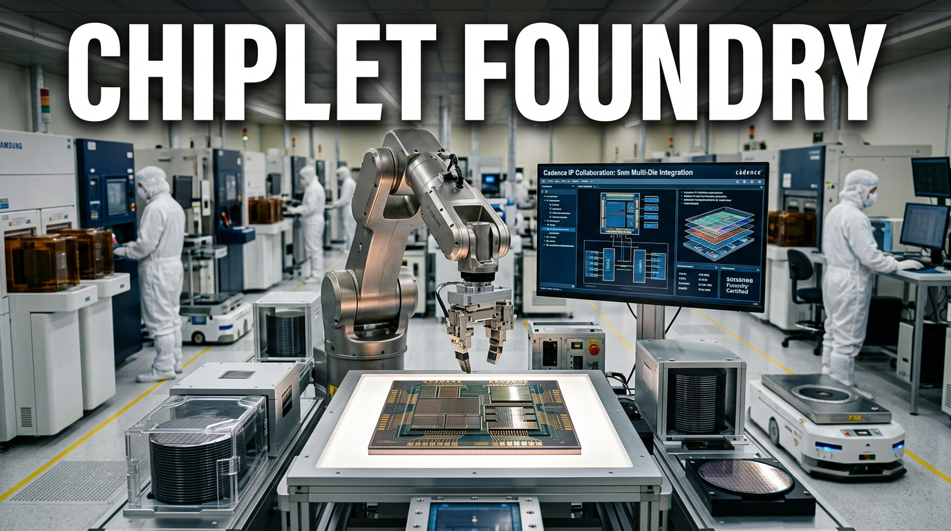
- Samsung Electronics and Cadence are scheduled to tape out a chiplet platform semiconductor for physical AI early next year.
- This chip will be based on a 5nm foundry process, and a physical product could emerge in the second half of next year.
- The key point is that it is not a single product, but a platform-type AI semiconductor that can be adapted for multiple industries.
- It targets demand for robotics semiconductors, autonomous driving, industrial automation, and drone control.
- Through this business, Samsung Electronics is building a foundation to attract more global fabless customers.
Why Is Samsung Electronics Entering Physical AI Semiconductors Now?
1. Because AI Has Moved Beyond the Screen
Physical AI refers to the stage where AI no longer operates only within digital screens,but instead controls actual devices and movements.
Robots moving their arms,cars judging road conditions,drones adjusting flight paths in real time,and factory equipment optimizing itself—all of these fall under this category.
In such environments, semiconductors are needed that can deliverlow power consumption,real-time computing,high-performance control,and multi-sensor connectivity, beyond ordinary AI chips.
Ultimately, the semiconductor market is expanding beyond data centerstoward edge AI and AI inference chips that move the real world.
2. The Next Battleground in Foundry Is ‘Platformization’
Until now, the basic foundry formula was relatively simple.
Customers designed their own chips,and foundry companies such as Samsung Electronics or TSMC manufactured them according to process requirements.
But this time, the industry is moving one step further.
Together with Cadence,Samsung Electronics is creating a platform chip that pre-implements 60 to 80 percent of the core functions,while customers add the functions they need to complete the product.
This meansshorter semiconductor production time,lower design costs,and faster commercialization of customized customer products.
Foundry competition is shifting from “who can manufacture better” to“who can provide a better-prepared platform.”
Why Chiplets Matter: A Game Changer for the Semiconductor Industry
1. Chiplets Are a ‘Divide and Build Better’ Approach
Instead of building one large chip all at once, chiplets are a technology that connects multiple dies divided by function and uses them as one system.
For example,CPU,NPU,memory interfaces,and key blocks such as PCIe are individually optimized,then connected during the packaging stage.
The advantages of this approach are quite clear.
- It offers greater design flexibility.
- It makes it easier to add functions.
- It accelerates customized development.
- It may be advantageous for yield management.
- It enables faster response to changes in AI semiconductor demand.
2. Why It Fits Physical AI Well
Physical AI has vastly different requirements depending on the use case.
Robotics requires real-time control,autonomous driving requires safety and sensor fusion,and industrial automation requires long operating hours and reliability.
Since it is difficult to satisfy all of these with a single chip,a chiplet-based structure is far more efficient.
In other words, Samsung Electronics’ choice of chiplets is not simply following a trend,but can be seen as a decision tailored to the structural characteristics of physical AI semiconductors.
The Significance of the Samsung Electronics–Cadence Partnership
1. Cadence Is a Key Player in EDA and the IP Ecosystem
Cadence is a company with strong influence in EDA and IP.
Put simply,it provides the tools and building blocks needed when designing semiconductors.
In this collaboration, Cadence supplies the IP needed for the platform,while Samsung Electronics optimizes it for foundry manufacturing.
This structure is highly important.
Why? Because in the semiconductor industry,how well IP and process work together ultimately determines product launch speed and competitiveness.
2. A Multi-Year IP Collaboration Contract Is Already in Place
The two companies already signed a multi-year IP collaboration agreement in June of last year.
In other words, this announcement is not a sudden one-off partnership,but the concrete realization of a pre-planned ecosystem strategy.
From an investor’s perspective, this is quite important.
Compared with short-term event-driven news,it is more likely to lead to actual production and customer acquisition.
The Most Important Point in This Article, and What Other Reports Often Miss
1. The Shift From ‘Selling Chips’ to ‘Selling Platforms’
Many reports stop at saying, “Samsung Electronics is making AI semiconductors.”
But the core takeaway is much bigger.
Going forward, Samsung Electronics is moving away from a structure where it produces chips one by one for customers,and toward providing a pre-validated semiconductor platform.
This also affects the revenue model.
Once a platform is established,one design can expand across multiple industries,and switching costs for customers rise,which makes it advantageous for securing long-term foundry clients.
2. ‘5nm Process’ Is Not Just a Number, but a Matter of Trust
It is also important that this platform will use Samsung Electronics’ 5nm process.
5nm is more than a sign of advanced miniaturization;it is an indicator of yield stability and production reliability.
Especially for customers,the most important question when adopting a new platform is whether it can be mass-produced stably with that process.
Therefore, this business is not only a battle of technology,but also a proving ground for foundry productivity and yield competition.
3. Physical AI Structurally Expands Semiconductor Demand
While data center AI had strong demand centered on a few big tech companies,physical AI spreads across the entire industrial sector.
That means it can extend toautomotive,robotics,drones,manufacturing,logistics,and healthcare.
In other words,the AI semiconductor market could shift into a much larger pie.
That is why Samsung Electronics’ move should be read not merely as a new product launch,but as a strategy to preempt future semiconductor demand.
Changes to Watch From an Economic and Industrial Perspective
1. Reshaping the Foundry Competitive Landscape
If Samsung Electronics releases a platform-type physical AI semiconductor,foundry competition becomes more complex.
This is because competition is no longer just about process nodes,but also about platforms, IP, packaging, and ecosystems.
Through this process, Samsung Electronics may strengthen its image beyond being a memory semiconductor leaderand position itself as a core player in the AI semiconductor supply chain.
2. Lower Barriers to Entry for Fabless Customers
Platform-based semiconductors are quite attractive for fabless companies.
Instead of designing everything from scratch,they can add only the necessary functions on top of a proven base platform.
This is especially beneficial for startups and small to mid-sized fabless firms.
As a result, Samsung Electronics may attract not only large customersbut also the fast-growing AI fabless customer segment.
3. Positive Spillover for Korea’s Semiconductor Ecosystem
This trend is not limited to Samsung Electronics alone.
It can connect toEDA,IP,advanced packaging,design services,and system semiconductor startups.
In other words, it can be seen as a signal that Korea’s semiconductor industry is expanding from a memory-centric model to one centered on system semiconductors and AI semiconductors.
Upcoming Schedule and Key Points to Watch
1. Tape-out Schedule Early Next Year
Tape-out is the stage where design is completed and handed over to manufacturing.
If this stage proceeds as planned,the project moves one step closer to actual mass production.
2. Whether Physical Products Launch in the Second Half of Next Year
Typically, mass production takes time after tape-out.
Based on this article, a launch could come after roughly six months,so the platform chip may actually emerge in the second half of next year.
3. Who Will Be the First Customer?
Ultimately, the biggest question is the first customer.
Whether it is a robotics company,an automotive company,or an industrial automation firmwill shape market perception.
Securing the first customer will serve as the barometer for whether this platform truly has market potential.
4. The Speed of Chiplet Ecosystem Expansion
It is also important to see what other IP partners join alongside Cadence.
Chiplets are not something one company can succeed with alone;design, packaging, verification, and process all have to align.
Therefore, how quickly the ecosystem expands will likely determine the success or failure of the business.
Points That Investors and the Industry Should Watch Together
- Check whether it aligns with the period when the foundry industry is recovering.
- Confirm whether AI semiconductor demand turns into actual orders rather than just expectations.
- 5nm process yield and production stability are key.
- Chiplets and advanced packaging competitiveness are likely to become even more important.
- Whether Samsung secures global fabless customers could determine its medium- to long-term growth potential.
In Summary, the Real Meaning of This News
Samsung Electronics’ move is not merely a new semiconductor business.
It shows the shift of the center of gravity in AI semiconductors from data centers to the physical world,and Samsung Electronics is attempting to preempt that change from the centerwith platform foundry.
In particular, the chiplet-based structureenables faster customized production,so it could have major significance in the markets for robotics semiconductors, autonomous driving semiconductors, and industrial automation semiconductors.
In the end, the real point of this news is not that“Samsung Electronics is making AI semiconductors,”but that“Samsung Electronics is changing the very way AI semiconductors are made.”
< Summary >
Samsung Electronics plans to tape out a chiplet-based physical AI semiconductor platform with Cadence early next year.
This platform is a customized AI semiconductor architecture that can be expanded for robotics, autonomous driving, drones, and industrial automation.
The core point is not simple production, but the evolution into platform-based foundry, with 5nm process competitiveness and chiplet ecosystem expansion as key points to watch.
[Related Articles…]
- The KOSPI 8000 era has opened… Why Samsung Electronics and SK hynix led the way
- Chinese humanoid companies expand contact points in Korea… concerns over low-price offensives
*Source: https://v.daum.net/v/y9LPakJ6Ie