● Silicon Photonics Shakes Up the AI Connectivity War
Why Silicon Photonics Is Opening the Second Act of AI Semiconductors: After GPU Competition Comes the “Connectivity” War
The core point of the AI semiconductor market is now shifting from a simple race to secure GPUs to “how quickly, with how little power, and how reliably data can be moved.”
In this article, we will examine in news style why silicon photonics is emerging as a technology to solve the bottleneck in AI data centers, how it connects with competition in GPU, HBM, NVLink, and TSMC packaging, and what impact it may have on the semiconductor industry and the global economic outlook.
In particular, the core point often missed in other articles or videos is not that “light is fast,” but that the economics of AI systems can no longer be made to work with copper wires alone.
In simple terms, the coming competition in AI infrastructure is likely to be a comprehensive battle that is no longer about GPU performance alone, but about data center power costs, advanced packaging, optical transmission, yield, and maintenance.
1. The first act of AI semiconductors was the race to secure GPUs; the second act is competition over “connectivity infrastructure”
So far, the first act of the AI semiconductor market has been about how many NVIDIA GPUs can be secured.
Major cloud companies and big tech firms have made massive capital expenditures to secure large quantities of high-performance GPUs such as H100, H200, and Blackwell.
But the more GPUs are deployed, the bigger a new problem becomes.
That problem is the speed and power consumption of data movement between GPU and GPU, GPU and memory, server and server, and rack and rack.
As AI models grow larger, not only does computation increase, but data movement also explodes.
When data movement is slow, no matter how many good GPUs you buy, overall system performance does not come out properly.
That is why the second act of AI semiconductors is not “computation” but “connectivity.”
Silicon photonics is rapidly emerging as the core technology to solve this connectivity bottleneck.
2. What is different between optical communication and silicon photonics?
Optical communication itself is not a new technology.
It has long been used in internet backbone networks, undersea cables, and telecom networks to send data as light over distances from several kilometers to thousands of kilometers.
Even the high-speed internet we use at home or in the office is largely delivered through fiber-optic infrastructure.
But the recently spotlighted silicon photonics is a little different.
The core idea is not optical communication connecting distant cities, but a movement toward connecting very close chips to chips, boards to boards, and even within servers and racks, using light.
Traditionally, it was natural to connect short distances with copper wires.
Because the distance is short, there was no need to go through the complexity of converting everything to light.
But in AI data centers, speed and power issues have become serious even over distances of a few dozen centimeters or a few meters.
Now, the industry broadly recognizes that even at short distances, copper-based transmission is reaching its limits.
3. The core principle of silicon photonics: a technology that “carries” electricity on light
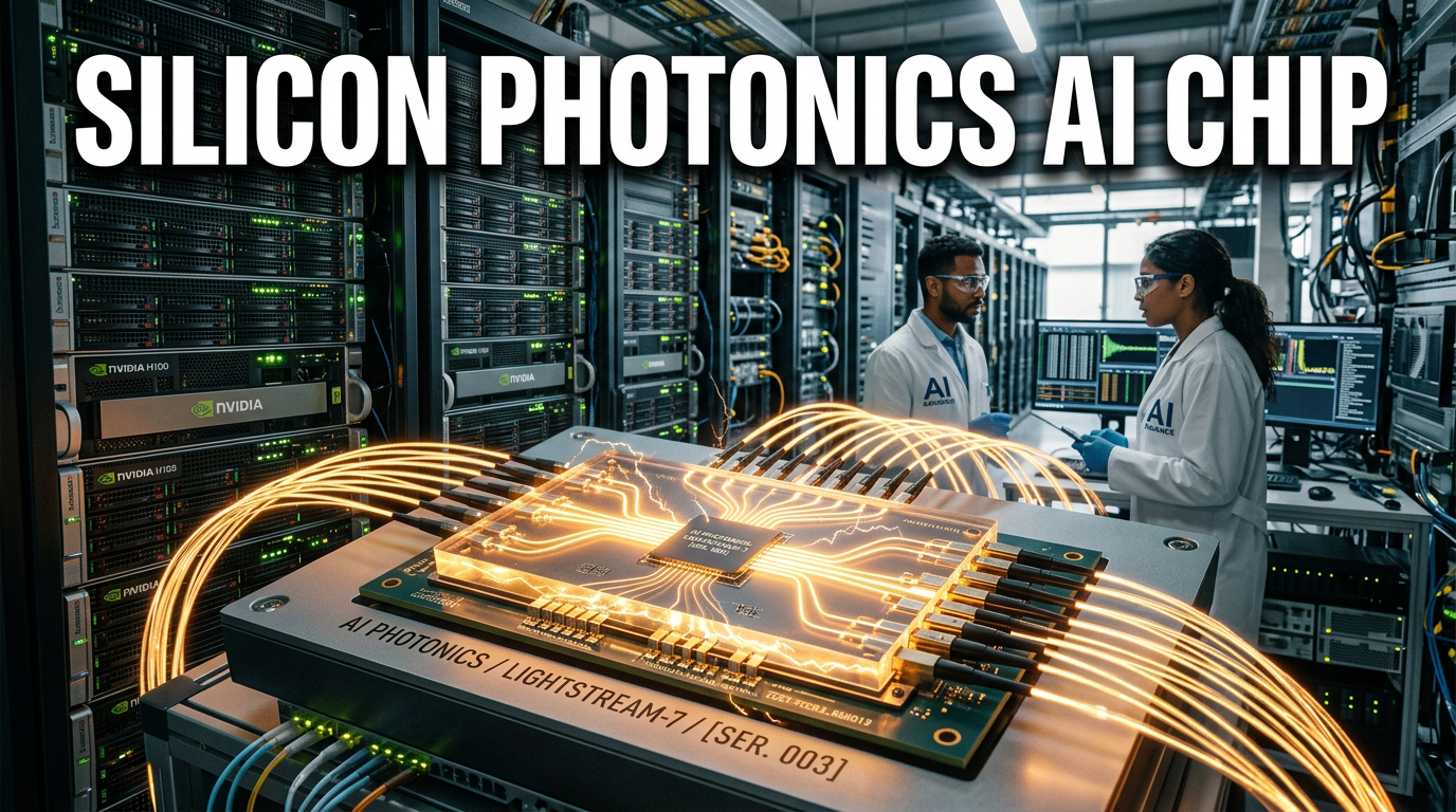
Silicon photonics, as the name suggests, is a technology that handles light on a silicon chip.
The important point here is that silicon photonics is not a technology that creates light from nothing.
Typically, continuous light from an external laser, that is, light carrying no signal, is received by the silicon chip.
Then the light moves along a path called a waveguide formed on the silicon chip.
A waveguide is literally a channel through which light passes.
Semiconductor devices such as PN diodes are placed around this channel, and electrical signals are applied to them.
When the 0s and 1s digital signals from AI semiconductors such as GPUs, NPUs, and TPUs are applied to these semiconductor devices, the state of the traveling light changes.
This process is called modulation.
In simple terms, it is the process of imprinting 0s and 1s data onto light that originally had no information.
The light carrying that data then moves through optical fiber or optical waveguides to other chips or modules.
On the other side, that light is converted back into electrical signals so the semiconductor chip can understand it.
4. Why has silicon photonics suddenly become important now?
Silicon photonics is actually a technology that has been researched for 30 to 40 years.
The technology itself did not appear completely new.
Even so, the reason it has not become mainstream until now is simple.
Copper wires were too convenient, too cheap, and too stable.
Electrical signals can simply be connected with wires.
But to use light, a transmitter that converts electrical signals into optical signals is needed.
And on the receiving side, a receiver that converts optical signals back into electrical signals is also needed.
In other words, extra chips, packaging, assembly processes, alignment technology, and test costs are added in the middle.
Because of these burdens, the industry wanted to keep using copper wires as long as possible.
But AI has changed the game.
To train and infer with ultra-large AI models, thousands or tens of thousands of GPUs must move like one giant computer.
At this time, if data exchange between GPUs is slow, overall performance drops sharply.
In the end, silicon photonics is changing from a “nice-to-have technology” into a “technology that, if not used, runs into system limits.”
5. The limits of copper wires: more frightening than speed is power and heat
Copper wires are still powerful over short distances.
But when data speeds rise above hundreds of Gbps and the number of connected chips increases explosively, the problem changes.
When current flows through copper wires, heat is generated due to resistance.
As distance and speed increase, more power is needed to maintain signal quality.
In data centers, that power is a direct cost.
Power is not only used to run servers; it is also consumed again for cooling the heat that is generated.
That is why the power issue in AI data centers is not merely a technical issue but a matter of operating costs and profitability.
By contrast, when light travels through optical fiber, there is in principle almost no heat generated by electrical resistance.
Of course, energy is required to turn on the laser, modulate the signal, and receive it.
But in high-speed, large-capacity data transmission, the zone where optical transmission becomes more power efficient than copper is expanding rapidly.
Park Young-jun, CTO of LIFAC, explained that if light-based transmission is introduced into data centers, an energy saving of roughly 30 to 40 percent is being discussed overall.
This figure may vary depending on the actual system structure and scope of application, but the direction is clear.
As power costs rise sharply in AI data centers, silicon photonics is both a performance technology and a cost-reduction technology.
6. How silicon photonics changes the economics of AI data centers
AI infrastructure investment can no longer be evaluated simply by how many GPUs were purchased.
The truly important question is how much computation can be handled stably in the same amount of power and space.
When silicon photonics is introduced, data center economics can change in three major ways.
First, GPU utilization can rise.
GPUs are expensive assets.
But if bottlenecks in data movement cause GPUs to spend a lot of time waiting, investment efficiency falls.
Reducing bottlenecks through optical transmission can reduce GPU idle time and raise the efficiency of the entire cluster.
Second, the burden of power costs and cooling costs can be reduced.
One of the biggest bottlenecks in AI data centers is power infrastructure.
If power efficiency improves, more AI servers can be operated within the same contracted power capacity.
Third, the freedom of server design can increase.
Copper wires have short high-speed transmission distances and make signal-loss management difficult.
Optical transmission can enable high-speed transmission over relatively longer distances, allowing more flexible design of server, rack, and cluster structures.
7. The competitive landscape between existing laser methods and silicon photonics
Although silicon photonics is attracting attention, it would be hard to say that it will monopolize all optical transmission.
In conventional optical communications, the method of directly modulating light by applying electrical signals to the laser itself has been widely used.
This method has a lot of operational experience and is relatively simple in structure.
From a laser manufacturer’s perspective, existing technology can be advanced to address the AI short-distance transmission market.
By contrast, silicon photonics modulates continuous light from a laser on a silicon chip.
Because it is silicon-based, it can leverage semiconductor process experience and has advantages in mass production and integration.
Silicon also has the advantages of reliability and relatively low cost.
However, silicon photonics still carries major challenges in packaging, optical alignment, yield, thermal management, and testing.
In the end, the market is likely to develop in a way where existing direct-modulation laser methods and silicon photonics compete while also complementing each other.
8. The connection between NVLink, PCIe, UCIe, and optical transmission
NVIDIA’s NVLink is a key interconnect technology for high-speed GPU-to-GPU connections.
Even in the Blackwell generation, NVLink and NVLink Switch are evaluated as core elements that determine the performance of large-scale GPU clusters.
However, current connections within GPUs and between adjacent chips still mainly rely on copper-based transmission.
In the future, efforts to extend digital signals in the form of NVLink into optical transmission may continue.
PCIe is also a representative standard for connecting CPUs, GPUs, accelerators, and storage devices inside servers.
UCIe is drawing attention as an open interface for chiplet-to-chiplet connections.
As AI semiconductors increasingly move toward chiplet structures and advanced packaging, the trend of combining optical transmission on top of these electrical interfaces may become important.
In simple terms, future AI systems will compete not only on which chip is faster, but also on which connection standard and which optical transmission structure they adopt.
9. Why TSMC is drawing attention: light ultimately enters packaging
TSMC is frequently mentioned as one of the most important companies in silicon photonics.
The reason is simple.
In the AI semiconductor era, how chips are packaged and connected has become as important as how well they are made.
TSMC has already secured a strong position in the advanced packaging market.
Its role continues to grow in the trend where GPUs, HBM, interposers, chiplets, and high-bandwidth connections are combined inside one package.
Optical transmission is also likely to move closer and closer into the packaging structure, rather than remaining a separate component attached outside the chip.
This trend is commonly called CPO, or Co-Packaged Optics.
CPO is an approach that places the optical engine close to the switch or processor package to shorten the distance traveled by electrical signals and improve power efficiency.
As CTO Park Young-jun mentioned, TSMC is likely to occupy an important position in silicon photonics structures and packaging direction.
In the end, optical technology cannot win alone; it must move together with semiconductor processes, packaging, and customer system design.
10. Intel’s position: strengths in mass production experience with silicon photonics, but structure and yield remain variables
Intel is often mentioned as the company with the longest record of tangible achievements in silicon photonics.
Intel has long supplied silicon photonics products for communications.
Mass production experience is a very large asset in this market.
There is a huge gap between what works in the lab and what is actually supplied in large volumes as a product when it comes to optical technology.
However, short-distance optical transmission inside AI data centers has different requirements from the traditional long-distance communications market.
Price, power, yield, packaging location, assembly difficulty, and maintenance methods all differ.
CTO Park Young-jun explained that while Intel’s approach is technically excellent in some areas, there may be yield-related difficulties in certain structures.
This means that the market is likely to move beyond simply “who did it first” and toward “who provides the structure best suited to AI systems.”
11. From the perspective of Samsung Electronics and SK Hynix: the next connectivity technology after HBM
Silicon photonics is also a very important key takeaway from the perspective of the Korean semiconductor industry.
SK Hynix has secured a strong position in the HBM market and has emerged as a core company in the AI semiconductor supply chain.
Samsung Electronics is a company with capabilities in memory, foundry, packaging, and system semiconductors.
In the first act, where the AI semiconductor market grew around GPUs and HBM, HBM competitiveness was important.
But in the second act, it becomes more important how HBM is attached to GPUs, how GPU clusters are connected, and how overall system power efficiency is improved.
At this point, advanced packaging and silicon photonics become connected.
For Korean companies, long-term competitiveness cannot be guaranteed by being good only at HBM.
They must be able to provide customers with a combined package of HBM, interposers, chiplets, optical transmission, packaging tests, and thermal management.
12. The point highlighted by LIFAC: what is harder than the technology itself is “optical packaging”
LIFAC, where CTO Park Young-jun works, is a company focused on technology that packages light, as its name suggests.
This part is quite important.
The key challenge of silicon photonics is not merely handling light on a silicon chip.
To make a real product, the laser, silicon photonics chip, electronic chip, optical fiber, substrate, package, and thermal management structure must all be combined precisely.
Light is more difficult to handle than electricity.
Electrical signals can be connected relatively easily with metal wiring, but light is sensitive to position, angle, and alignment errors.
Even a slight mismatch can cause significant loss.
Equipment entering AI data centers must not fail, and even if it does fail, it must be able to be replaced quickly.
That is why optical packaging is not simply an assembly technique, but the core bottleneck in commercializing silicon photonics.
LIFAC has focused on applying fan-out wafer-level packaging, or the FOWLP family of approaches used in semiconductor packaging, to optical packaging.
If chips, lasers, and the necessary electronic circuits are precisely placed and connected in wafer form, opportunities may arise in terms of mass production and precision assembly.
13. Are the EUV light of ASML and the light of silicon photonics the same light?
There is a point that many people confuse.
The question is whether ASML’s EUV equipment and silicon photonics use the same technology since both use light.
In principle, they are the same in that both use electromagnetic waves, namely light.
But industrially, they belong to completely different areas.
ASML’s EUV is lithography equipment used to draw semiconductor circuits at extremely small scales.
EUV has a wavelength of about 13.5 nm, which is extremely short.
By contrast, the lasers used in communications and silicon photonics are typically in the several-hundred-nm to 1,300-nm and 1,550-nm ranges.
In other words, EUV is the light that makes chips, while the light of silicon photonics is the light that sends data between chips.
Both are essential to the semiconductor industry, but their roles, technical difficulty, and supply chains are different.
14. The most important point that other news coverage often misses: the real battleground for silicon photonics is not “light” but “system cost”
When discussing silicon photonics, explanations often end with “light is fast” and “power efficiency is good.”
But the truly important point is elsewhere.
First, the total cost of ownership of AI systems changes.
This is no longer an era that looks only at the price of GPUs; total cost including power, cooling, network equipment, maintenance, and fault response becomes competitive.
Silicon photonics is a technology that can shake this total cost structure.
Second, the standing of packaging companies rises further.
This is not a market where chip designers alone can succeed.
Where to place the optical engine, how to make wiring shorter, how to remove heat, and how to replace parts in the event of failure all matter.
That is why the value of TSMC, Samsung Electronics, OSAT, optical component companies, and substrate companies can all be re-evaluated together.
Third, the power infrastructure of data centers can determine the speed of AI investment.
In the United States, Europe, Korea, and Japan, securing power for AI data centers is a major issue.
If grid expansion is slow, it is difficult to rapidly expand data centers even if GPUs are purchased.
Silicon photonics, which improves power efficiency, can become a key variable in AI infrastructure investment strategy.
Fourth, the winner is likely to come not from a single technology company, but from an ecosystem combination.
Laser companies, silicon photonics companies, foundries, packaging firms, cloud companies, and AI semiconductor designers all need to move together.
This market is not one where making one good product is enough; it is a market where the side that controls standards and supply chains has the advantage.
15. From the perspective of the global economic outlook: AI infrastructure investment will continue, but the direction of money will change
In the global economic outlook, AI remains a core growth axis.
However, if the investment focus in 2023 to 2024 was centered on GPU shortages and HBM shortages, future funds are likely to move toward areas that solve bottlenecks in data center infrastructure.
Representative areas include power infrastructure, cooling systems, network semiconductors, optical components, advanced packaging, and high-speed interconnects.
As AI semiconductors become more advanced, bottlenecks keep shifting.
At first GPUs were insufficient, then HBM was insufficient, and later packaging capacity and power infrastructure became problems.
Now data movement and connectivity structures are emerging as important bottlenecks.
From an investment perspective as well, it is no longer enough to simply say “NVIDIA is good”; the entire AI data center value chain must be considered.
The semiconductor industry is increasingly becoming a systems industry, and silicon photonics is a representative technology showing that transition.
16. Checkpoints to watch from an investment perspective
The first checkpoint is the timing of actual adoption.
Silicon photonics is promising, but it is not a technology that will immediately enter all data centers on a large scale.
Adoption speed may vary depending on the size of the AI cluster, transmission distance, power costs, and maintenance costs.
The second checkpoint is packaging yield.
Optical technology has high alignment and assembly difficulty.
If yield is low, price competitiveness falls no matter how good the performance is.
The third checkpoint is standardization.
It is important how it combines with the interconnect ecosystem such as NVLink, PCIe, UCIe, Ethernet, and CXL.
The fourth checkpoint is the measured effect of power savings.
A 30 to 40 percent energy saving is being discussed, but the actual savings rate will vary depending on the system structure and scope of application.
Therefore, in company announcements, one should verify system-level power efficiency rather than simply performance figures.
The fifth checkpoint is customer adoption.
In this market, actual adoption by hyperscale data center customers matters more than technology demos.
Which structure the Microsoft, Google, Amazon, Meta, and OpenAI-related infrastructure ecosystems choose can determine the direction of the market.
17. How silicon photonics will change the semiconductor industry structure
In the future, semiconductor competitiveness will be difficult to explain with process miniaturization alone.
Of course, advanced processes such as 2nm and 3nm will continue to be important.
But in the AI era, the ability to bundle multiple chips and make them operate like one system is becoming more important than the performance of a single chip.
In this process, advanced packaging, HBM, optical transmission, network chips, and power management semiconductors all become important together.
Silicon photonics is at the center of this trend.
That is because it can connect GPUs and HBM faster, reduce data bottlenecks between servers, and improve the power efficiency of data centers.
In the end, the core question in the second act of AI semiconductors is not “who makes the fastest chip?”
Going forward, “who can build the most efficient AI system?” is likely to become more important.
18. The core structure at a glance
Existing structure: Connections between GPUs, memory, and servers are handled mainly through copper-wire-based electrical signals.
Problem: As data speeds increase, signal loss, power consumption, heat generation, and distance limitations grow.
Silicon photonics structure: Electrical signals are carried as light on a silicon chip and sent via optical transmission.
Expected effect: High-speed transmission, improved power efficiency, lower data center operating costs, and higher GPU utilization are possible.
Core challenges: Optical packaging, yield, alignment, testing, maintenance, and standardization are key issues.
Main player group: TSMC, Intel, Samsung Electronics, SK Hynix, NVIDIA, optical component companies, packaging specialists, and data center operators are all connected.
< Summary >
The AI semiconductor market is moving beyond the race to secure GPUs and into competition over data movement and connectivity infrastructure.
Silicon photonics is drawing attention as a core technology to solve the speed, power, and heat limits of copper-based transmission.
This technology uses light on a silicon chip to carry digital signals and transmit data quickly between chips, servers, and servers.
In AI data centers, power and cooling costs are rising, so a structure based on optical transmission can play an important role in improving economics.
However, the real battleground for silicon photonics is not the light itself, but packaging, yield, maintenance, standardization, and customer adoption.
Going forward, the core of the semiconductor industry is likely to shift from the performance of a single GPU to the efficiency of the overall AI system that combines GPU, HBM, packaging, and optical transmission.
[Related Articles…]
AI Semiconductor Market Outlook and the Next-Generation Packaging Race
AI Data Center Power Infrastructure and Global Investment Strategy
*Source: [ 티타임즈TV ]
– 왜 실리콘 포토닉스가 AI 반도체의 2막을 여는가 (박영준 라이팩 CTMO)