● 400C OLED
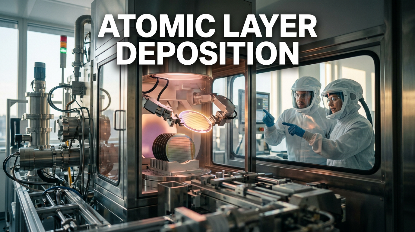
“Breaking Through ALD’s Limits, ‘Semiconductor Process at 400°C or Below’”…the Real Change that ‘ALG’ from Jusung Engineering Brings
1) The Core Point of Today’s News: Why Is ‘ALG (Atomic Layer Growth)’ Drawing Attention Now?
In this interview, the most important core point is exactly three things.
First, ALD (Atomic Layer Deposition) has significantly lowered the temperature of semiconductor processes, but
the next step—trying to directly control thinner, more precise thin films through a “growth” approach—is that ALG is the answer.
Second, ALG is not merely a “thin-film coating technology,”
and it is described in a direction that makes it possible at low temperatures for the transistor channel (the path where current flows) and for road/connection lines (wiring/interconnects) and even the capacitor.
Third, once this low-temperature process becomes possible, the message was strong that in “industries that must stack layers, like semiconductors,” process design freedom will grow, and as a result, stacked-expansion efforts like HBM and next-generation device paradigms could be accelerated.
2) First, a Clean Summary: Differences Between ALD and ALG (Deposition vs Growth)
The analogy used in the interview to help people understand ALD and ALG was quite intuitive.
(1) ALD = Deposition, “a way where snow piles up”
ALD is the concept of “coating” materials on the surface in ultra-thin layers at the atomic-layer level.
The analogy emphasizes the direction of building up—like how, when snow falls, it piles up layer by layer.
This approach has strengths for large-area and precise thin films, but we also have to see that in next-generation miniaturization, there is a point where more precise structure control/performance limits become evident.
(2) ALG = Growth, “a way where ice freezes in 3D”
ALG was explained not as simple deposition, but as something closer to controlling in a 3D way—starting from the surface—what kind of “ice” is formed in what shape.
In other words, it is an idea aimed at controlling more directly “even with the same material, what kind of quality/structure/characteristics the resulting thin film forms.”
Consequently, if designers can create the desired ‘ice (thin film) shape,’ there is a greater chance that, in the next generation of semiconductor processes, performance, yield, and cost can all be addressed together.
3) Why It’s Needed Now: The Collision Between Process Temperature and Miniaturization
This is where a semiconductor process challenge appears squarely.
Semiconductors are becoming increasingly miniaturized, and they must stack more layers and combine a wider variety of materials.
(1) Problems with existing high-temperature processes: “‘1000°C-class’ becomes poison for the later stack”
In the past, processes like CVD (Chemical Vapor Deposition) involved flows that required high temperatures (1,000°C or more),
and the context is that as the side effects that occur there accumulated, process complexity increased.
(2) Even dropping to the “300–400°C range” wasn’t the end
ALD contributed to lowering temperatures roughly from 1,000°C to 400°C, but
in the next generation, it’s not only the transistor channel—
wiring (roads), capacitors (storage devices), and stacked structures must all be solved within the same low-temperature framework.
There was a particularly important warning in the interview.
When making a transistor channel, using high temperature briefly is possible,
but wiring/capacitor processes build up once and then again and again—so if you raise the temperature, the roads melt and collapse.
4) The True Bottleneck ALG Tries to Solve: Keep Channel-Wiring-Capacitor at the Same Low Temperature
Among the interview content, the clearest part of the technical direction is the logic that “if materials and the process change, you can keep stacking layers.”
(1) The ‘technology’ to create the channel: using better-performing materials (III-V)
Until now, transistor channels have mainly been built on single-crystal silicon,
and there was discussion that when miniaturization and high-performance requirements grow, materials in the III-V family (e.g., gallium nitride, gallium arsenide) could be advantageous.
The issue, though, was “how to grow that III-V in the cheapest way, where, and at what temperature.”
(2) The Key Keyword of This Generation: Low-temperature (400°C class) to even ‘glass substrates’
The interview takes one step further from here.
If, at 400°C or below, you can grow III-V on ‘glass’ or create structures equivalent to that,
it suggests that unit cost, scale, and application range could change dramatically.
This becomes the starting point of a story that extends not only to semiconductors but also to solar power/displays.
(3) A ‘pipe (channel)’ concept that also connects to Gate-all-around (GAA)
In the interview, they explained transistors as “water flowing in a pipe (channel),”
and gate-all-around is connected as a structure that wraps around the pipe’s circumference to control current flow more precisely.
The key message is that, beyond the structure itself, precise material/thin-film quality is essential for that structure to work.
5) The Ripple Effect Spreading to Solar Power, Displays, and Semiconductors: “A Game of Growing Materials Cheaply”
The interview expands the idea that “ALG is not just a technology that changes semiconductor processes.”
(1) Solar power: the bottleneck wasn’t efficiency—it was ‘cost/mass production’
III-V-based solar power mentions efficiency (e.g., 35% or higher), but
the flow in the past was that commercialization was limited because it was too expensive and hard to mass-produce.
If an ALG/low-temperature growth foundation is introduced,
they built expectations that manufacturing costs could be reduced by more than 100x, enabling mass production and expanding adoption.
(2) Displays: lowering the wall where transistor and light-emitting layers used to be separated
In displays, materials for transistors (driving) and materials for emission (OLED, etc.) are generally separated, and the processes differ.
The interview presents the view that “if integrated fabrication using one material/one technology becomes possible,”
it could lead to manufacturing simplification + price decreases (they even mention a possibility of up to 30x).
(3) Semiconductors: potential linkage with stacked scaling (including HBM)
HBM is a representative area of “stacking layers to increase bandwidth.”
In the interview, they left room for possible ALG application, but they summarize that “how many layers will be stacked is determined by the design/the business.”
In other words, ALG has a strong character as a foundational technology that makes stacking layers possible.
6) The Reality of Commercialization Timing: Equipment/process are ready, but ‘design technology’ needs further evolution
This is the most practically oriented part you can hear.
There was a nuance that some equipment/processes for ALG are already at a mass-production readiness level, but
ultimately, they emphasize that full-scale spread happens when a market-fit product (design/architecture) is combined.
Semiconductors are not “done with materials/process alone”—circuit design, foundry, and product design have to align.
7) The Interview’s Perspective: “Semiconductors are city design”…Korea is strong only in “buildings,” but weak in “city design”
The famous metaphor that came up here is quite important from an investment/industry perspective.
The frame is that in semiconductors, circuit design (city design) determines success or failure, and process/equipment/materials are closer to the infrastructure that allows building that city.
The interview included self-assessment/suggestions that Korea may be strong in building block/component/device manufacturing capabilities, but
from the standpoint of designing the entire electronic circuitry/system (city design), it may have developed relatively less.
This part can also be read as meaning that once process technologies like ALG exist, the next question is “what design will be built on top of it, and who will make money.”
8) Separate Summary (the ‘single most important line’ that doesn’t often appear in other articles)
The essence of ALG is not ‘deposition,’ but an attempt to control the 3D quality/structure of thin films more directly through ‘growth,’ and then bring the results—beyond just the transistor channel—into low-temperature processing as far as wiring/capacitors and stacked layers.
Once you understand this one line, everything connects at once—why the technology extends into semiconductors, solar power, and displays.
Main Points to Convey (Checklist)
- From ALD (deposition) to ALG (growth): evolving from “stacking thin films” to “controlling how the thin film forms”
- In miniaturization, the key challenge is temperature constraints: channel/wiring/capacitor must all fit into a low-temperature framework
- Potential to use III-V (e.g., gallium nitride/gallium arsenide): room for performance improvement + extending to glass substrates
- For solar power, the bottleneck is ‘cost/mass production’ rather than ‘efficiency’: with a low-temperature growth foundation, a paradigm shift could be possible
- Displays have potential to lower process separation barriers: expectations for manufacturing simplification and cost reduction
- Possible linkage with stacked scaling such as HBM: design (circuit/product) needs to evolve along with it
- Industry perspective: the value is completed only when process/materials (infrastructure) and circuit design (city design) move together
Blog SEO Keywords (naturally inserted)
Today’s content especially matches readers’ search intent with keywords like semiconductor processes, atomic layer deposition, next-generation semiconductor materials, low-temperature thin-film growth, and HBM.
< Summary >
ALG was introduced as a next-generation process direction that goes beyond ALD’s limits of ‘atomic layer deposition,’ aiming to control thin films more precisely through a ‘growth’ method.
The core is that at 400°C class low temperatures, III-V materials (e.g., gallium nitride) could be applied even to glass substrates, enabling low-temperature stacking not only of transistor channels but also of wiring and capacitors.
The ripple effects could extend to semiconductors (including HBM), solar power (mass production and cost reduction), and displays (simplified manufacturing integration), but for full-scale commercialization, the key is ultimately the combination with ‘design technology.’
[Related Articles Words…]
- Next-generation semiconductor process changes through ALG
- Key points in process/materials behind HBM stacking competition
*Source: [ 티타임즈TV ]
– 주성엔지니어링의 ALG 기술이 주목받는 이유 (황철주 회장)