● Silicon Photonics Shake Up AI Chips with Light Based GPU Computing
Silicon Photonics Shakes Up GPUs: The Next Battleground in the AI Semiconductor Race Is Light and Packaging
The real point to focus on here is not simply “sending data faster with light.”
The key takeaway is whether silicon photonics can move beyond data transmission and even handle the computations that GPUs used to perform.
If that becomes possible, it could shake up the AI semiconductor market, data center power costs, HBM placement structures, semiconductor packaging strategies, and even South Korea’s semiconductor cluster policy all at once.
In particular, what matters in Park Young-jun, CTMO of LIFAK, is not that “silicon photonics will immediately replace GPUs,” but that the bottleneck in AI infrastructure is shifting from computation to data movement, and the possibility of light breaking through that bottleneck is growing.
1. News Core Point: AI semiconductor competition is expanding from GPUs to optical semiconductors
- Key figure:
Park Young-jun, former professor in Seoul National University’s Department of Electrical Engineering and current CTMO at LIFAK, explained the strategic significance of silicon photonics.
- Key technology:
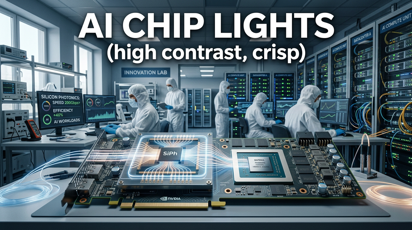
Silicon photonics is a technology that uses light instead of conventional electrical signals to transmit data between chips, between boards, and ultimately within systems.
- Key change:
The current AI semiconductor race is no longer just about GPU performance; it has become a systems competition that includes HBM, semiconductor packaging, glass substrates, optical transmission, and data center power efficiency.
- Key outlook:
If silicon photonics solves transmission, that would be a major revolution; if it also solves computation, it would be a “revolution within a revolution.”
2. What Is Silicon Photonics: A Technology That Breaks Through Electron-Limited Paths with Light
In conventional semiconductor systems, electrons move data through copper wires.
But as AI models grow larger, the amount of data that must move between GPUs, HBM, network equipment, and servers explodes.
The problem is that while electrical signals are fast, they have limits in terms of distance, heat, power consumption, and latency.
Silicon photonics introduces light into this path.
Using optical signals instead of electrical ones makes it possible to transmit data at much higher speeds and can also improve power efficiency.
As power costs have become one of the biggest bottlenecks in AI data centers, silicon photonics is not just a semiconductor technology but also an economic technology that reduces energy costs.
3. Why Silicon Photonics Matters Now: The Bottleneck in the AI Era Is Changing
Early AI semiconductor competition was about “who can build a more powerful GPU.”
But now there is a problem that matters just as much as GPU compute performance.
That is how quickly data can be fetched, how quickly it can be moved, and how little power it takes to process it.
AI models continuously exchange enormous amounts of data during training and inference.
No matter how fast the GPU is, if data is fetched slowly from HBM or moved slowly between servers, overall performance declines.
That is why AI semiconductor competition is shifting from a standalone GPU race to an infrastructure race that combines GPUs, HBM, networks, packaging, and optical transmission.
4. The Biggest Point: If Silicon Photonics Can Handle GPU Computation, the Game Changes
The strongest message Park, CTMO emphasized was that if silicon photonics can perform the calculations GPUs do using light, it would be a revolution within a revolution.
GPUs are fundamentally structures in which transistors perform multiplication and addition at tremendous speed.
The core of AI computation is large-scale matrix operations, where multiplication and addition repeat continuously.
However, in silicon photonics-based structures, researchers are studying ways to arrange light paths like X and Y axes and use the nonlinear properties of certain materials so that computation occurs where light meets.
Put simply, it is the concept of letting light replace part of what electrons used to compute.
In theory, this could drastically reduce power consumption and raise speed to a different level from conventional electron-based circuits.
Of course, many challenges remain before commercialization.
Temperature sensitivity, system stability, manufacturing cost, mass production, and integration with existing semiconductor processes still need to be solved.
But HBM was not originally predicted to become the superstar of the AI era either.
Just as HBM, which began with demand from gaming graphics, emerged as a core memory in the generative AI era, silicon photonics could also rise sharply when market demand aligns with it.
5. The Synergy Between HBM and Silicon Photonics: It May No Longer Be Necessary to Keep Memory Only Next to the GPU
In today’s AI accelerator architecture, HBM is tightly attached right next to the GPU.
The reason is simple.
To move data quickly through copper wires, the components need to be physically close.
But once optical transmission becomes possible, this structure could change completely.
If data can travel rapidly by light, there is less need to keep memory right next to the GPU.
In that case, it may become possible to configure large-scale memory farms inside data centers.
For big tech companies like Meta, Microsoft, and Google, being able to place memory more flexibly could significantly improve infrastructure efficiency.
That is because they could distribute memory resources more efficiently to where they are needed, rather than attaching expensive HBM only in limited amounts next to GPUs.
For South Korea, this is extremely important.
Korea already has global competitiveness in HBM, and if silicon photonics changes the HBM connection structure, it can create new added value.
This creates an opportunity to move from being simply a country that excels at making HBM to one that provides AI semiconductor system solutions combining HBM and optical transmission.
6. The Shift in Semiconductor Packaging: What Used to Be a “Secondary Process” Is Now the Battleground
In the past, semiconductor packaging was often viewed as a back-end process for packing and connecting chips.
But in the AI semiconductor era, packaging has become a core technology that determines performance.
One reason TSMC maintains its powerful position in the global foundry market is its advanced packaging competitiveness.
AI semiconductors are not completed by a single chip alone.
GPU, HBM, logic chips, I/O chips, optical transmission modules, and more must all work together like a single system.
Some chips require cutting-edge sub-2nm processes, while others may not need such advanced nodes at all.
What matters is the overall design capability to determine how to combine them, where to connect them with copper, and where to connect them with light.
Semiconductor packaging is no longer just assembly; it is system architecture.
In particular, once silicon photonics enters the picture, “where to place the optical component,” “how to connect it with HBM,” and “how to arrange the GPU and optical module” become core sources of competitiveness.
7. Glass Substrates and Silicon Photonics: Not a Substitution Relationship, but a Combinable Technology Pair
Recently, glass substrates have also been drawing major attention in the semiconductor industry.
Compared with conventional organic substrates or silicon interposers, glass substrates have advantages in certain areas.
They have lower electrical loss, are favorable for large-area implementation, and also have potential from a cost perspective.
Rather than being in direct competition, silicon photonics and glass substrates can be combined.
Because glass has good optical transmission properties, it can be used by incorporating optical waveguides inside the substrate.
In other words, a glass substrate can become more than a simple support panel; it can become an advanced packaging platform that includes a path for light.
That said, glass substrates also have drawbacks.
They are fragile, difficult to process, and must achieve reliability in mass production.
Still, companies including Corning are conducting glass-substrate-based demos, and rapid technological progress is appearing in some areas.
8. What It Means for South Korea’s Semiconductor Industry: Gwangju, the Honam Region, and Non-Capital-Area Clusters Can Seize a New Opportunity
Park, CTMO, explained that Korea already has some talent and industrial foundation related to optics.
In particular, policies that once fostered the optical industry centered on Gwangju may gain new significance in the age of silicon photonics.
At the time, optical technology had not yet fully entered the mainstream of the IT industry, so there were not many cases of growth into large enterprises.
But in the AI semiconductor era, optical transmission, optical packaging, and silicon photonics are emerging as core technologies.
The foundation built 20 years ago now has the potential to finally shine.
The important thing is not simply building more memory fabs.
What is needed is a specialized cluster that brings together optical semiconductors, semiconductor packaging, chiplet design, and system architecture.
Just as Taiwan has Hsinchu and China has Shenzhen, Korea also needs a regionally specialized semiconductor cluster strategy.
9. The Core Point of Government Policy: It Must Nurture “People” and “Architecture,” Not Just Equipment or Factories
Park, CTMO, pointed to one regret in Korea’s past semiconductor policy: the gap in silicon semiconductor research and talent development.
There was a view that since companies were doing well, the government had nothing to do, and as a result there was a period when silicon semiconductor fields weakened in universities and research projects.
Semiconductors are an industry that requires long-term talent development.
If there are no professors, graduate students are hard to produce; if there are no graduate students, there is a shortage of advanced talent entering companies and research institutes.
AI semiconductors, silicon photonics, glass substrates, and advanced packaging are all fields that require long-term investment in people.
In particular, future demand will favor talent who can see the whole system rather than those who only know individual devices well.
What is needed are architecture-type experts who can understand chip design, materials, transistors, packaging, optical transmission, and data center structure together and propose optimal solutions.
10. After Moore’s Law: Competing Only by Making Things Smaller Is Not Enough
In the past, semiconductor performance improvements were often achieved by making processes smaller and finer.
But as Moore’s Law approaches its limits, it has become difficult to solve performance and power issues through miniaturization alone.
Process scaling requires enormous investment, and the technical difficulty rises sharply as well.
That is why the industry is looking for other ways to improve performance.
Chiplet structures, advanced packaging, HBM, silicon photonics, and glass substrates are all part of the same trend.
Making things smaller is still important, but so is connecting them well, arranging them well, and building structures that consume less power.
11. The Real Core Point That Other News Often Misses: Korea’s Risk Is Not Only a Lack of Technology
Many articles and videos focus on the technical potential of silicon photonics.
But the sharper point in Park, CTMO’s remarks is the global customer anxiety about Korea’s semiconductor supply chain.
Korea has a very high global market share in key memory semiconductors, especially HBM and DRAM.
That is a strength for Korea, but at the same time it is a risk from the perspective of global customers.
If dependence on a specific country is too high, they cannot help worrying about geopolitical risk, production disruptions, labor issues, and the possibility of supply interruptions.
What matters here is not how many trillions of won Korean companies lose when a factory stops.
The bigger issue is the damage suffered by customers.
If AI data centers and big tech companies experience supply disruptions, they begin looking for alternative supply chains.
Once a customer leaves, they do not easily come back.
In other words, Korea’s real competitiveness in semiconductors includes not only technology but also stable supply trust, the continuity of clusters, talent supply, and the labor system.
Global competitors in the AI era are moving in ways that are less constrained by time.
If Korea regards the AI semiconductor industry as national core infrastructure, it must also think about system competitiveness that preserves production continuity and customer trust.
12. Silicon Photonics from an Investment Perspective: More Like a Long-Term Infrastructure Shift Than a Short-Term Theme
It is still too early to view silicon photonics as a technology that will replace all GPUs in the short term.
But as a candidate technology for solving bottlenecks in the AI semiconductor industry, it is very important as a long-term investment theme.
In particular, four areas deserve attention.
- First, optical transmission modules.
The demand for technology that can quickly move data between servers and between chips inside AI data centers is likely to grow.
- Second, HBM connection structures.
If HBM and GPUs can be connected more flexibly through optical transmission, the structure of the memory semiconductor market could change.
- Third, advanced packaging.
Because silicon photonics cannot be separated from packaging, the strategic value of advanced packaging companies could increase further.
- Fourth, glass substrates and optical waveguides.
If glass substrates evolve into platforms that include optical signal pathways, new demand for materials and equipment could emerge.
13. The Global Competitive Landscape: Could It Become the Key to Breaking Nvidia’s Dominance?
It is hard to say that silicon photonics will immediately replace Nvidia GPUs.
That is because Nvidia’s competitiveness includes not only the GPU chip itself but also the CUDA ecosystem, software, networks, system design, and customer lock-in structure.
But if silicon photonics becomes an essential technology for AI infrastructure, the situation changes.
Nvidia will also have to respond to changes in optical transmission and packaging, and companies such as TSMC, Samsung Electronics, SK hynix, Intel, Broadcom, and Corning could all enter the new competitive axis.
In particular, if optical transmission is commercialized first and optical computation becomes practical in some areas afterward, the AI semiconductor market could move even faster from a GPU-centric structure to a systems-centric one.
In that case, the winner is likely not the company that makes the single best chip, but the one that most efficiently integrates data movement, computation, memory, and packaging.
14. What Korea Should Do Now: Move from a HBM Powerhouse to an AI Semiconductor Systems Powerhouse
Korea holds a strong position in HBM and memory semiconductors.
But if AI semiconductor competition shifts into a systems competition, being good at memory alone may no longer be enough.
To move to the next stage, Korea needs three strategies.
- First, a strategy that views HBM and silicon photonics together.
Rather than only thinking about selling more HBM, Korea must consider how to place HBM within an optical-transmission-based system.
- Second, fostering specialized clusters for optical semiconductors and packaging.
Using the existing optical industry base in places like Gwangju and the Honam region, Korea needs clusters that combine optical semiconductors, advanced packaging, glass substrates, and chiplet design.
- Third, cultivating system architecture talent.
Universities, research institutes, and companies must work together to develop talent that can design the entire AI infrastructure, not just individual technologies.
15. Conclusion: Silicon Photonics Is Not a “Future Technology” but a Practical Solution Targeting the Bottlenecks of AI Infrastructure
Silicon photonics still has many problems to solve.
Price, stability, temperature sensitivity, mass production, and integration with existing semiconductor processes are all difficult issues.
But as power consumption in AI data centers and bottlenecks in data movement continue to intensify, semiconductor technology that uses light is becoming less of an option and more of a necessity.
If transmission shifts to light, the structure of AI semiconductors changes.
If even part of computation can be handled by light, the GPU-centered order could also crack.
For Korea, this is an important golden time to extend its HBM competitiveness into optical transmission and packaging.
In the future, semiconductor competition is likely to shift away from who makes the smallest chip and toward who makes the fastest and most efficient AI system.
At the center of that are silicon photonics, HBM, semiconductor packaging, glass substrates, and data center power efficiency.
< Summary >
Silicon photonics is a technology that transmits data with light instead of electricity.
In the AI semiconductor era, not only GPU performance but also data movement speed and power efficiency are key bottlenecks.
If silicon photonics solves optical transmission, that is a major revolution; if it handles even GPU computation with light, it could reshape the semiconductor market.
When combined with HBM, it makes possible a more flexible AI data center architecture that does not need to keep memory only next to the GPU.
Semiconductor packaging is no longer a secondary process but a core technology that determines AI system performance.
Glass substrates, when combined with silicon photonics, can become a next-generation packaging platform that includes optical signal pathways.
Korea must extend its HBM strengths into optical semiconductors, packaging, and system architecture.
Now is an important golden time for Korea to move into a leadership position in AI semiconductor systems.
[Related Articles…]
- How AI Semiconductor Market Shifts Are Reshaping Global Supply Chains
- How HBM Competition Is Changing Data Centers and the Memory Industry Outlook
*Source: [ 티타임즈TV ]
– “실리콘 포토닉스가 빛으로 GPU 연산을 대신한다면 혁명중의 혁명” (박영준 라이팩 CTMO)