● Yellow-Lit Semiconductor Secret, Yield Power, AI Chip Edge
Why Semiconductor Fabs Use Yellow Lighting: Its Link to Yield, Photoresists, and AI Chip Productivity
The “yellow room” in a semiconductor fab is not merely a matter of ambiance or worker eye protection.
It is a critical zone in the photolithography process, where lighting can affect chip defects and overall yield.
As demand for AI semiconductors accelerates and capital spending, global supply chains, and productivity competition intensify, even small process controls can affect corporate earnings and macro outlooks.
This article explains why yellow light is used instead of white light, how photoresists respond to light, and why lighting itself is part of yield management.
1. Where the Yellow Room Is in a Semiconductor Fab
Not every area in a semiconductor fab uses the same lighting.
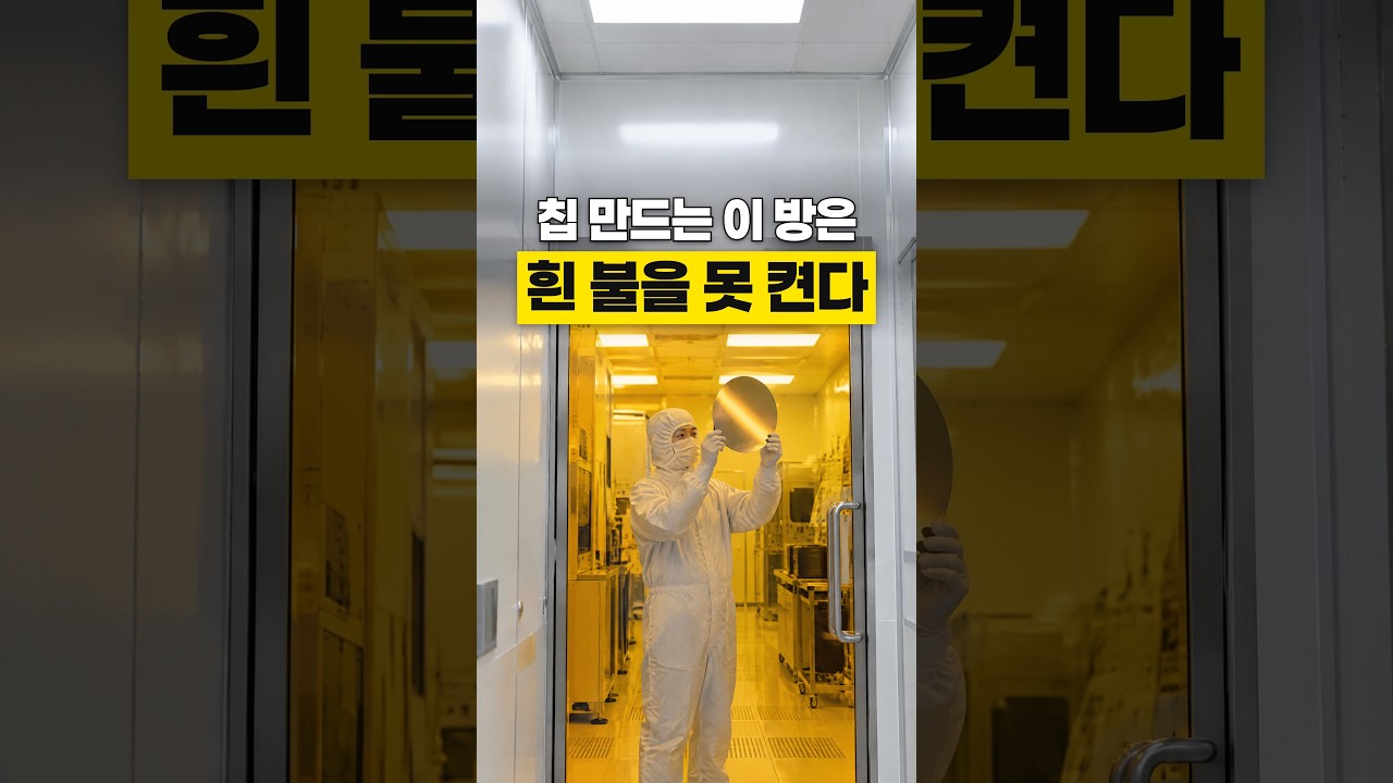
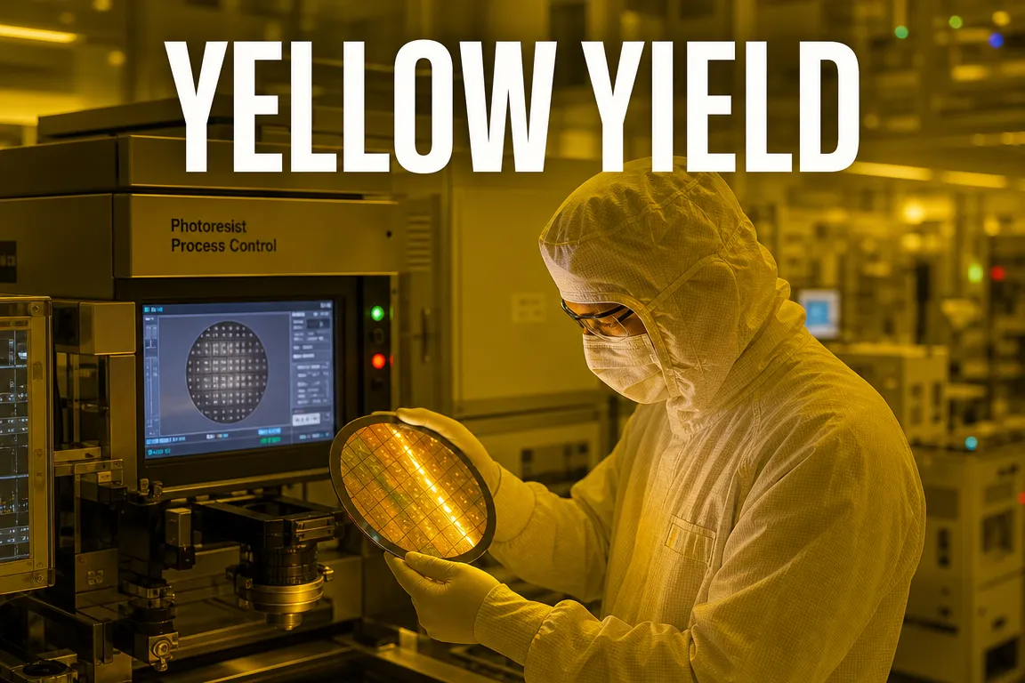
Yellow lighting is commonly used around photolithography areas where circuit patterns are transferred onto wafers.
This space is often referred to as a yellow room, amber-light area, or lithography zone.
The reason is straightforward: the materials handled there are highly sensitive to light.
Semiconductors are manufactured by repeatedly patterning ultra-fine circuits on wafers.
To form those patterns, a light-sensitive material called photoresist is applied as a thin coating.
Photoresist reacts not only to exposure-tool light but also to ambient light from overhead fixtures or windows.
2. Core Principle: Photoresist Changes Properties When Exposed to Light
Semiconductor patterning can be understood in a way similar to photographic printing.
Photoresist is coated on the wafer.
Light is then projected through a mask containing the circuit pattern.
Areas exposed to light and areas not exposed undergo different chemical changes.
Development then leaves the intended pattern on the wafer.
The key requirement is that only the intended areas change.
If white light from overhead fixtures reaches the photoresist, unwanted reactions can occur.
This can blur circuit edges, create unintended patterns, or distort critical dimensions.
In semiconductor manufacturing, even small errors become defects.
Lighting control is therefore part of yield management.
3. Why Yellow Light Is Used: Longer Wavelengths Carry Less Energy
Light differs by wavelength across colors.
Ultraviolet and blue light generally have shorter wavelengths and higher energy.
Yellow, orange, and red light have longer wavelengths and lower relative energy.
Photoresists are typically sensitive to higher-energy light such as ultraviolet or blue wavelengths.
When exposed to short-wavelength light, the resist undergoes chemical reactions that alter its properties.
Yellow light has relatively low energy and is less likely to alter photoresist.
Semiconductor fabs therefore filter out short-wavelength light and retain lighting that is effectively safe for the process.
Yellow lighting is not special in itself; it is the result of removing the wavelengths that can trigger unwanted resist reactions.
4. Why White Light Is a Risk: It Contains Multiple Wavelengths
White light appears clean and bright, but physically it contains a mixture of wavelengths.
That mixture includes blue-light components that can affect photoresist.
In some lighting environments, ultraviolet-like or other short-wavelength components can also be problematic.
In semiconductor manufacturing, “close enough” is not acceptable.
A single wafer can contain many chips, and advanced-process wafers carry high value.
If lighting causes unintended photoresist reactions, the quality of an entire batch can be affected.
Fab lighting is therefore equipped with yellow filters, and windows or work areas are designed to block short wavelengths.
5. Summary in News Style: Fab Lighting Is a Yield Investment, Not a Cost Item
Fact 1: Yellow lighting is primarily for protecting photoresist, not worker convenience.
In semiconductor production, yellow lighting is an environmental control measure designed to prevent unintended resist reactions.
Fact 2: White light can include short wavelengths that affect photoresist.
White light contains multiple colors, some of which have enough energy to alter the resist.
Fact 3: Yellow light is close to safe light for photoresist handling.
Yellow lighting reflects the removal of wavelengths to which photoresist is highly sensitive.
Fact 4: Lighting control is directly linked to semiconductor yield.
Minor pattern deviations can create defects, making lighting an important part of productivity management.
Fact 5: In the AI semiconductor era, process stability matters more.
For high-value products such as GPUs, HBM, and advanced logic chips, process miniaturization and yield control are central to competitiveness.
6. The Key Point Often Missed: The Yellow Room Is a Process Condition, Not Just a Color
Most explanations stop at the statement that photoresist reacts to light, so yellow light is used.
The more important point is that yellow lighting is one process condition among many.
Semiconductor production controls temperature, humidity, dust, vibration, chemical concentration, exposure time, development time, and even light wavelength.
Lighting is therefore a process parameter that affects yield.
Different photoresists also have different wavelength sensitivities.
Resist types used in i-line, DUV systems at 248nm and 193nm, and EUV-compatible processes each have distinct characteristics.
Fab lighting is therefore specified not simply as “yellow bulbs,” but in accordance with the resist and process requirements in use.
This is a point often overlooked in general coverage.
7. From an Economic Perspective: Yellow Lighting Is Hidden Semiconductor Competitiveness
Semiconductors are a capital-intensive industry that requires large-scale fabrication investment.
Building a leading-edge fab requires substantial capital, and the tools themselves are expensive.
However, profitability is not determined only by equipment purchases.
The real competitive edge lies in achieving stable high yield with the same equipment.
As AI chip demand rises, global supply chains are reorganizing around advanced manufacturing capacity.
Expanding data center investment and growing demand for GPUs and high-bandwidth memory are making semiconductor productivity directly linked to market power.
Companies that can control even minor variables such as lighting achieve lower defect rates and greater delivery stability.
The yellow room is therefore not just a visual feature of the fab; it is a symbol of cost competitiveness and profitability in semiconductor manufacturing.
8. Key Points for Investors and Industry Observers
First, semiconductor competitiveness comes from process detail.
Ownership of EUV tools and advanced packaging capabilities matters, but yield stabilization is essential in mass production.
Second, as the AI chip market expands, small process differences create large gaps.
More complex circuits and higher process difficulty make control of lighting, contamination, and environmental conditions increasingly important.
Third, global supply competition is not only about output volume.
The decisive factor is who can supply with higher yield and greater stability.
Fourth, in a capex expansion cycle, investors should also watch materials and process-control technologies.
Photoresists, filters, cleanroom systems, metrology tools, and process automation providers may all benefit from semiconductor investment.
9. One-Sentence Summary
Semiconductor fabs use yellow lighting instead of white light because photoresists can react to short wavelengths such as ultraviolet and blue light, which can distort circuit patterns.
Yellow lighting filters out those risks and helps protect wafers during processing.
This lighting control is directly linked to yield, productivity, AI semiconductor competitiveness, and supply chain stability.
[Related Articles…]
*Source: [ 월텍남 – 월스트리트 테크남 ]
– 반도체 공장 회로 찍는 방에 흰 불 대신 노란 불만 켜는 이유